This post is also available in: Türkçe
- What is SRAM?
- Why RAM is used with PIC?
- General Information about LH52256 and RAMs
- LH52256 MicroC Library and General Principle of its Circuit
- LH52256 SRAM Circuit
- LH52256 Circuit Scheme
- LH52256 SRAM MicroC Library
- CONCLUSION
- Library Files – Codes
- References
What is SRAM?
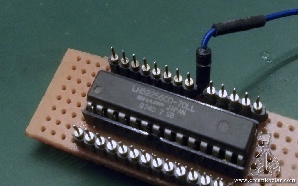
- SRAM aka static rams are high speed rams. Writing-reading speeds are at ns(nano second) level (1ns = 0.000000001 sn )
- The reason for the static ram name is:
- RAMs we attach to the computers are called as dynamic rams because there is a refreshing period in order to keep the information in it, so refreshing process is required. However, this is not necessary for static RAMs. The difference is related to this.
- These are generally used for processor support in computers. L1 and L2 memory determine the amount of SRAM while you get processor
- Although they are fast, their size is not as high as other DRAMs (general rams installed in computers). So it is preferred where high speed is required
- Due to RAM, the data is also deleted (as expected) when the power is turned off naturally.
Why RAM is Used With PIC?
- During my experiment, when a quick measurement is made, no matter how fast the HDD-SD Card is, it is still slow to write data, as everyone knows. And this causes the data to disappear. In general computer principle, the data is loaded into the RAM firstly, and then transferred it into the hard disks.
- PICs also have RAMs in certain sizes, but they are very few, and there is not much left other than general program.
- Unfortunately, while I was researching about this, I ran into some ridiculous information, such as the information that two PIC would only used for ram, rather than a real solution.
- The solution to overcome this problem is to use external RAM (not unnecessary use of extra PIC)
- I use it for the device I designed to measure the rocket engine power because I need to take a sample in 1/100 second to make a world standard rocket motor measurement. As you can see, there is no hard drive that can reach at this speed, because even though the writing speed is high, the hard drives have a communication confirmation procedure, which cause delay.
- I decided to use an external ram for the PIC because of the insufficient micro RAM. I chose the LH52256 SRAM, which has high speed and the size is pretty good compared to PIC.
General Information about LH52256 and RAMs
- First, let’s look at how ram size is calculated
- We are looking at how many “ADDRESS” pins RAM integration has
- There are 15 for LH52256 (A0-A14)
- For that, it means 215 = 32768. So, there are maximum 32768 addresses in RAM. (Note: each pin can be 1 or 0, then there are 2 possibilities. Therefore calculated as exponential function with base 2)
- Now I look at RAM “Input and Output (I/O)” ports
- The LH52256 also has 8 input and output. That is, 8 bits of RAM means that there is 32768*8 bit = 32768 bytes of space. If we say 32768/1024, RAM space equals 32 kbytes.
- NOTE: There may be different situations in some RAMs. Please check the manuals in detail, but in general SRAMs are like this.
- We are looking at how many “ADDRESS” pins RAM integration has
- I have calculated the size of the RAM, now let me calculate how many RAMs I need
- If we go from the above example, I need a system that will receive data from the sensor at 1/100 second interval and the data type is float.
- Float is 32 bit. That is 32768*8=262.144 bit. As float is 32 bit, that makes 262144/32=8192
- BeI was going to make a record in 1/100 seconds. Then 8192/100 = 81.92 seconds, so if I want to record in 1/100 second interval with 1 RAM and Float type, I can record 81 seconds. seconds.
- As you can see, I calculate the required RAM this way. I need 3-4 seconds to test the rocket motor, so this RAM is enough for the project.
LH52256 MicroC Library and General Principle of its Circuit
- As you will see later, and as I mentioned above, there are many pins in RAM. 15 address pins + 8 I/O pins and other feed control etc pins are available. It is not possible to connect all of them to the PIC.
- For this reason, I went through this problem by adding a shift register to the address space. That is, when the addressing is done in series, I connected the data part directly to the PIC in parallel format to avoid data loss in writing.
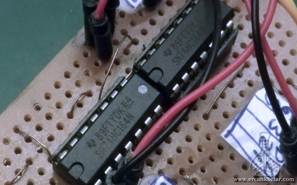
- I used 74HC164 for Shift Register. Let me explain briefly the working ration of these parts:
- Shift registers generally provide pin-saving. That is, they changes the serial input into parallel outputs
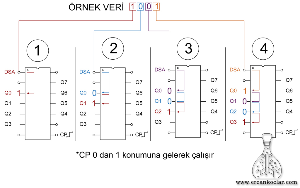
- It lines up one and zeros over PIC through only 1 pin on the outputs of its own. So when we spend a single pin on the PIC we set our data as parallel.
- When data is entered into the Shift Register, the CP tip located in itself is pulled down to zero so that the process is repeated everytimei and data is loaded.
- By examining the following visuals, you can grasp a little bit more information..
- Apart from all these, a lot of RAM’s pins can be used collectively. Because the CE (chip enable) pin is available. Therefore, whichever RAM is selected, it will be active, so many RAMs can be connected to the same address and data line.
- Since 4 RAM is used in general, I drew the circuit in this way, this number of RAM can also be increased. However, remember that for each RAM the CE tip will also be added.
LH52256 Pin Functions
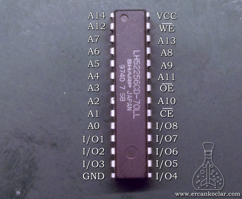
| Pin Name | Function |
| A0 – A14 | Address Entry |
| CE | Selects RAM |
| WE | Writing Function |
| OE | Reading Function |
| I/O1 – I/O8 | Data Input and Output |
| Vcc | Feeding +5V |
| GND | Grounding |
- In the above photo, some lines will appear on the pins. Line on a pin means that it is active at the low level (state 0).
74HC164 Pin Function
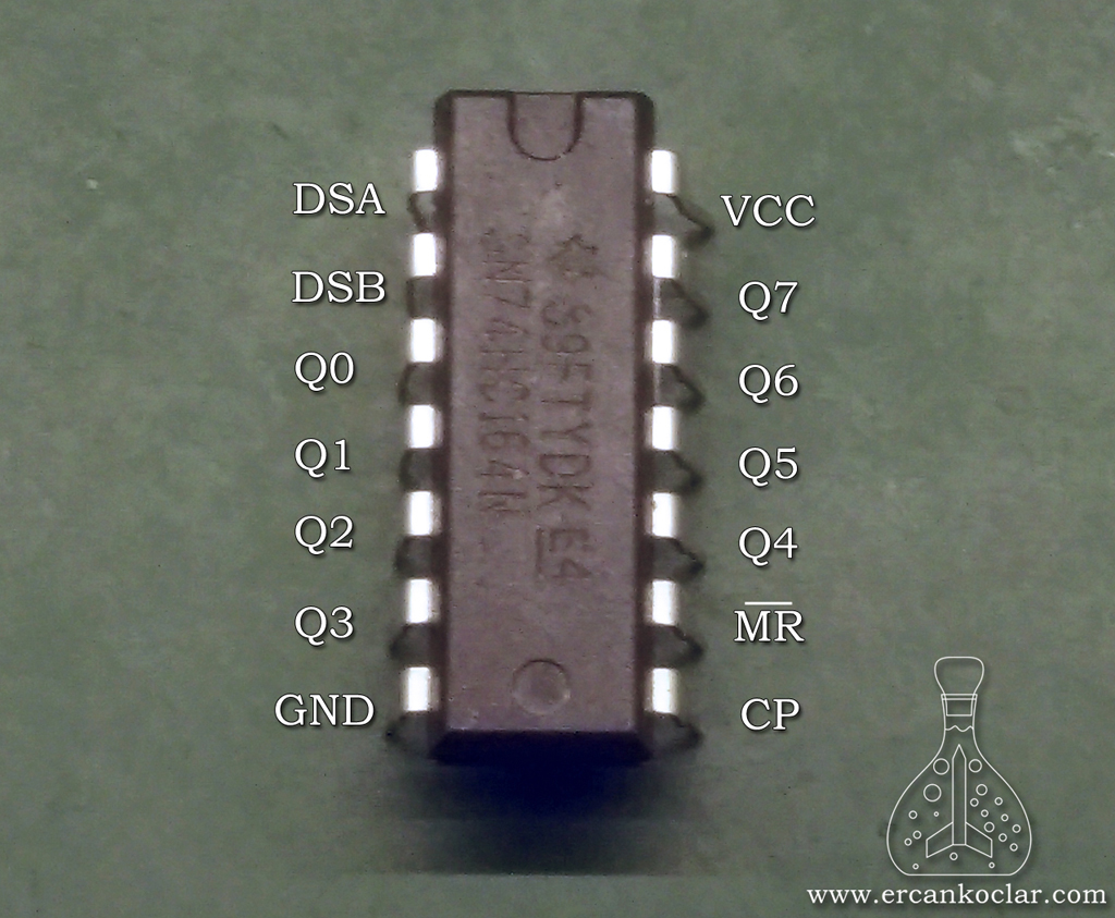
| Symbol | Pin | Description |
| DSA | 1 | Data Input |
| DSB | 2 | Data Input |
| Q0 – Q7 | 3,4,5,6,10,11,12,13 | Output |
| GND | 7 | Grounding |
| CP | 8 | Clock Pulse |
| MR | 9 | Master Reset |
| Vcc | 14 | Feeding +5v |
- In the study, I connected the DSB to the pole +5v directly, and made the control only from the point of DSA.
- CP runs from low to high (0 to 1)
- The MR pin is active at the low level and deletes all the data in the output.
LH52256 Running Protocols
- We will see the necessary steps to follow when using the LH52256.
- Note that the data will be erased when power is turned off in RAM integrations. The data is stored if there is energy
General Worksheet
| CE | WE | OE | Mode | I/O1-I/O8 | Feeding |
| H | x | x | Idle | High Level | 0.6 mA |
| L | H | L | Reading | Data Output | 25 mA |
| L | H | H | Output Cancellation | High Level | 25 mA |
| L | L | x | Writing | Data Input | 25 mA |
- The x sign indicates that it is not a matter of 0 to 1 in that case.
- Difference between Idle and Exit cancellation status; In idle mode, wake up of RAM takes longer (nano seconds, of course) but in this case less current is used. In the event of Output Cancellation, the RAM is ready to process but takes more current
LH52256 Data Reading Function
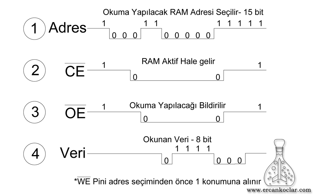
- WE pin is taken to position 1 before process starts
- Previously we calculated that LH52256 had a total of 32768 addresses, as 0-32767. In other words, we can give a value between 0 and 32767 as an address regardless it is in an order or not. Addresses help you choose the points that information is hidden
- The CE pin is pulled from 1 to 0, so that RAM is active. (If there is more than one RAM, the CE tip of the RAM should be activated, and the other RAMs should always be in position 1, otherwise it will have errors.)
- The OE pin is pulled down to 1, and it is reported that it will do reading.
- 8 bits of data are read from the I/O tips after all the above processes
- After reading, the operations are reversed and the RAM is returned to the initial position.
LH52256 Data Writing Process
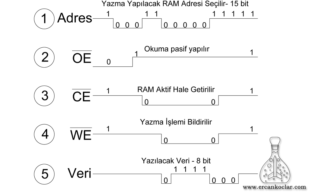
- First, the address to write is selected again
- Reading is turned off by taking OE tip back from 0 to 1
- RAM is activated by pulling CE tip back to 1.
- WE tip will be pulled back to 0 from 1, to inform that the Writing Operation should be performed
- After this process, 8 bits of data from the I/O point are written in the selected address
- Immediately after the write operation, the operations are reversed and the RAM is returned to the initial state.
LH52256 SRAM Circuit
- Since the circuit is for trial purposes, it was installed on a pertinax board.
- Since RAMs have common parts such as address and data pins and you will find it difficult to make them flat, I prefer to stick with the sockets as you will see below.
- Although I had 3 sockets, I made my experiments with 2 RAMs.
- Number of RAMs can be increased as desired.
- I used the 74HC164 shift register for addressing.
- Be sure to use sockets for RAMs or follow soldering instructions in the operating instructions.
LH52256 Circuit Scheme
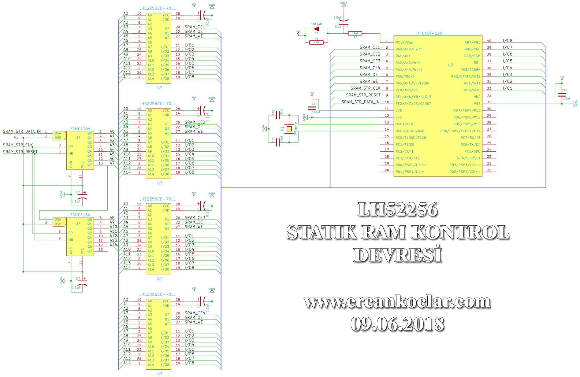
- Address – Input/Output – OE – WE tips are connected together and only CE tips are seperated.
- Since there are 15 addresses in the RAM, two 74HC164 are used.
- Address data from PIC comes in series with 74HC164, and goes to RAMs in parallel format
- Input-Outputs are directly connected to PIC
Necessary Materials
- 2 pcs 74HC164 shift registry integration
- 2 pcs 14 pin integration socket (for 74HC164)
- 4 pcs LH52256 SRAM integration (or 1 piece preferably)
- 4 pcs narrow type 28 pins integration socket
- 6 pcs 0.1uf condenser
- Pertinax
- Percision female and male sockets ( may differ according to circuit)
Making Circuit
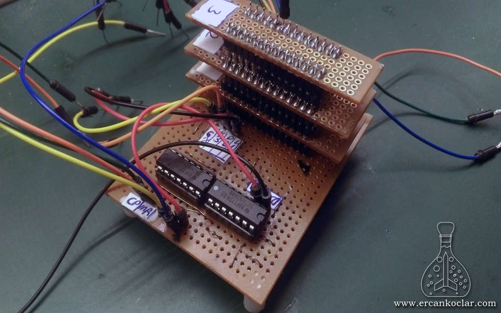
- RAM apartment is seen above :)
- The test circuits are more regular when the RAMs are stacked on top of each other.
- 2 integration on the front side are 74HC164.
- Soldering output and input pin cables can reduce the errors that occur in the working sequence.
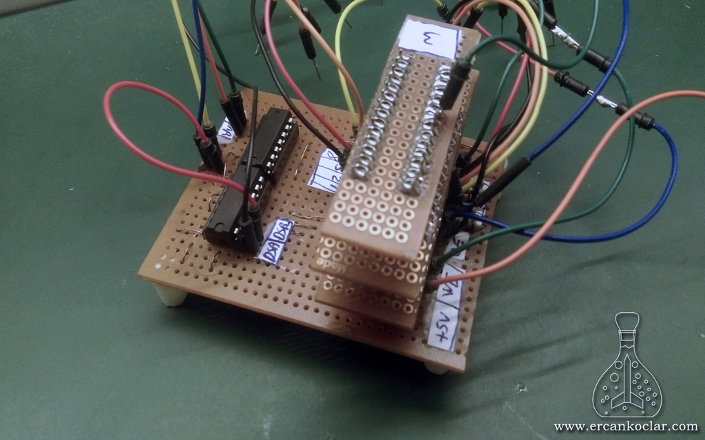
- You can see the tips behind the circuit.
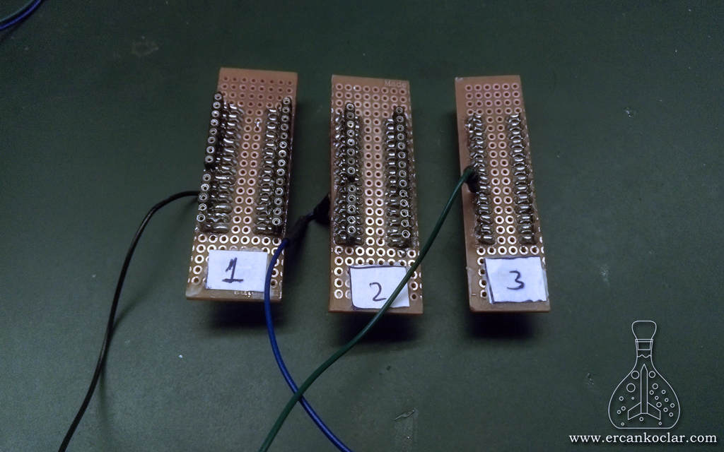
- The RAM sockets are numbered and the CE terminals are connected to the PIC via separate cables.
- In order to avoid confusion during the experiments, every socket is numbered.
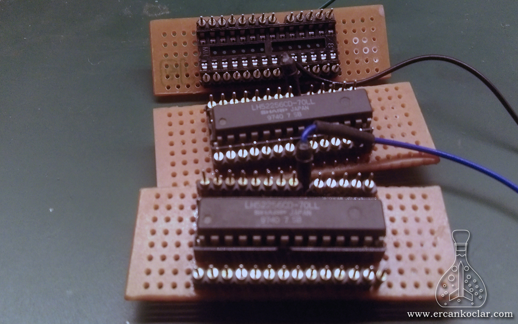
- You can see the insertion of RAMs.
LH52256 SRAM MicroC Library
- The LH52256 SRAM control library I wrote for MicroC is open source and can be run in other compilers with minor changes.
- Other SRAMs similar to the LH52256 are available. With simple modifications to the code, these RAMs can be used, or more RAM can be added to the system to do so.
Functions
- Now let’s examine the functions one by one
- User-oriented functions are indicated in green, system functions are indicated in red color.
- Be careful that operating the system functions in the usual way can cause errors.
- After briefly describing the functions, detailed examples will be given.
Shift Register Functions
– LH52256_RESET_RUTINI Function
Function: void LH52256_RESET_RUTINI()
Purpose : Deleting all previously written data on the 74HC164 makes the outputs “0“. Deletes address information
Parameters : N/A
How to Use :
LH52256_RESET_RUTINI();
Feedback : being in void type does not provide feedback
– LH52256_SHIFT_REGISTER_VERI_GONDERME_RUTINI Function
Function : void LH5225_SHIFT_REGISTER_VERI_GONDERME_RUTINI(unsigned char VERI)
Purpose : Provides data to be uploaded to 74HC164
Parameters :
- VERI : Informs whether data is 0 or 1
How to Use :
LH5225_SHIFT_REGISTER_VERI_GONDERME_RUTINI(1);//loads into shift register lojik 1 data, therefore next port lojik is 1
Feedback : Being in void type does not provide feedback
– LH52256_ADRES_SECMEFunction
Function: unsigned char LH52256_ADRES_SECME (unsigned int RAM_ADRESI)
Purpose: The LH52256 allows address selection in SRAM.
Parameters:
- RAM_ADRESI: The RAM address to be read is written here.
How to Use:
LH52256_ADRES_SECME(125);// SRAM in 125. address is selected
Feedback:
- If 0 is received, the address has been exceeded, ie the last address in LH52256 is 32767. If a value larger than this value is entered, it gives an error code because there is no such address.
General SRAM Functions
– LH52256_ANALIZ Functions
Functions: unsigned char LH52256_ANALIZ()
Purpose: Analyzes installed RAM and makes initial pin-port adjustments
Parameters : N/A
How to Use:
LH52256_ANALIZ();//RAMs in the system are analyzed
Feedback:
- Informs the number of RAM in the system.
– LH52256_RAM_SECME Function
Function : void LH52256_RAM_SECME(unsigned char RAM_NUMARASI)
Purpose:
- Arranges selection about which RAM will be used for operation
- Four RAMs can be defined in the software, but you can increase the number by changing the codes.
Parameters:
- RAM_NUMARASI: The RAM number to be processed is written.i.e: 1 ,2,3,4 etc.
How to Use:
LH52256_RAM_SECME(4);//The RAM which is inserted into 4th socket is activated.
Feedback : Since it is void type, it does not provide feedback.
– LH52256_DERINLEMESINE_TEST Function
Function: unsigned char LH52256_DERINLEMESINE_TEST(unsigned char RAM_NUMARASI)
Purpose: Controls all addresses of the selected RAM individually
Parameters:
- RAM_NUMARASI : The RAM to be deeply examine is selected
How to Use:
LH52256_DERINLEMESINE_TEST(2);//The RAM with socket number 2 performs an in-depth review
Feedback:
- If 0 is received, it means that there are errors in an address in the RAM
- If 1 is received, there are no errors in RAM addresses
SRAM Data Writing Functions
– LH52256_RAM_VERI_YAZMA_RUTINI_SABIT Function
Function : void LH52256_RAM_VERI_YAZMA_RUTINI_SABIT(unsigned char VERI)
Purpose: Writes 8 bit data
Parameters:
- VERI: It loads 8 bit data
How to Use:
LH52256_RAM_VERI_YAZMA_RUTINI_SABIT(125);
Feedback: Since it is a void type, there is no feedback.
– LH52256_RAM_VERI_YAZMA_RUTINI_ARTTIRIMLI Function
Function: void LH52256_RAM_VERI_YAZMA_RUTINI_ARTTIRIMLI(unsigned char VERI,unsigned char *HATA)
Purpose: Writes 8 bits of data and automatically increases the address one time
Parameters:
- VERI: 8 bits of data are loaded
- *HATA: Error flag:
- If Error Flag is read as”0“, that means address is exceeded.
- See how to use this flag to read
- This is also a pointer.
How to Use:
unsigned char abc;

LH52256_RAM_VERI_YAZMA_RUTINI_ARTTIRIMLI(125,abc);//While sending 125 data, the code to be received from pointer can be read from abc variable
Feedback: Since it is a void type, there is no feedback
– LH52256_RAM_VERI_YAZMA_RUTINI_AZALTIMLI Function
Function : void LH52256_RAM_VERI_YAZMA_RUTINI_AZALTIMLI(unsigned char VERI,unsigned char *HATA)
Purpose: Writes 8 bits of data and automatically reduces the address once.
Parameters:
- VERI: 8 bits of data is loaded
- *HATA: Error flag:
- If Error Flag is read as”0“, that means address is exceeded.
- See how to use this flag to read
- This is also a pointer.
- How to Use:
unsigned char abc;

LH52256_RAM_VERI_YAZMA_RUTINI_AZALTIMLI(125,abc);//When sending 125 data, the code that comes from the pointer can be read from the variable abc
Feedback: Since it is a void type, there is no feedback
SRAM Data Reading Functions
– LH52256_RAM_VERI_OKUMA_RUTINI_SABIT Fonksiyonu
Function: unsigned char LH52256_RAM_VERI_OKUMA_RUTINI_SABIT ()
Purpose: Reads 8 bits of data from RAM.
Parameters : N/A
How to Use:
unsigned char okunan_veri;

okunan_veri = LH52256_RAM_VERI_OKUMA_RUTINI_SABIT();
Feedback: Brings the value it read.
– LH52256_RAM_VERI_OKUMA_RUTINI_ARTTIRIMLI Function
Function: unsigned char LH52256_RAM_VERI_OKUMA_RUTINI_ARTTIRIMLI(unsigned char *HATA)
Purpose: Writes 8 bits of data and automatically increases the address one time
Parameters:
- *HATA: Error flag:
- If Error Flag is read as”0“, that means address is exceeded.
- See how to use this flag to read
- This is also a pointer.
How to Use:
unsigned char okunan_veri,abc;

okunan_veri = LH52256_RAM_VERI_OKUMA_RUTINI_ARTTIRIMLI(abc);
Feedback: Brings the value it read.
– LH52256_RAM_VERI_OKUMA_RUTINI_AZALTIMLI Function
Function: unsigned char LH52256_RAM_VERI_OKUMA_RUTINI_AZALTIMLI(unsigned char *HATA)
Purpose: Writes 8 bits of data and automatically reduces the address once.
Parameters:
- *HATA: Error flag:
- If Error Flag is read as”0“, that means address is exceeded.
- See how to use this flag to read
- This is also a pointer.
How to Use:
unsigned char okunan_veri,abc;

okunan_veri = LH52256_RAM_VERI_OKUMA_RUTINI_AZALTIMLI(abc);
Feedback: Brings the value it read.
Application of Functions
Pin Identification
- First, let’s look at pin identification
 sbit LH52256_CP   at RE0_bit;        //74164 Clock- clk
 sbit LH52256_DSA  at RE2_bit;        //74164 Shift register data is set here 1 or 0
 sbit LH52256_MR   at RE1_bit;        //74164 RESET
 char LH52256_DATA at portb;          //ram data I/O  entry
 sbit LH52256_CE1  at RA0_bit;        //ram1 chip enable
 sbit LH52256_CE2  at RA1_bit;        //ram2 chip enable
 sbit LH52256_CE3  at RA2_bit;        //ram3 chip enable
 sbit LH52256_CE4  at RA3_bit;        //ram4 chip enable
 sbit LH52256_WE   at RA5_bit;       //ram write enable
 sbit LH52256_OE   at RA4_bit;

 sbit LH52256_CP_Direction   at TRISE0_bit;
 sbit LH52256_DSA_Direction  at TRISE2_bit;
 sbit LH52256_MR_Direction   at TRISE1_bit;
 char LH52256_DATA_Direction at TRISB;
 sbit LH52256_CE1_Direction  at TRISA0_bit;
 sbit LH52256_CE2_Direction  at TRISA1_bit;
 sbit LH52256_CE3_Direction  at TRISA2_bit;
 sbit LH52256_CE4_Direction  at TRISA3_bit;
 sbit LH52256_WE_Direction   at TRISA5_bit;
 sbit LH52256_OE_Direction   at TRISA4_bit;
- I connected the LH52256 directly to a port since the data input/output is 8 bits. For this reason I made an identification as “char LH52256_DATA at portb“
- Since the LH52256 library works with a certain system, it is necessary to implement the operations in the proper order.
- This order is as follows:
- RAM Analysis
- Address Selection
- RAM Selection
- Reading and Writing Function
SRAM Analysis
void  main()
{
    unsigned char ram_sayisi=0;
    char txt[12];//required for circuit
    ADCON1=0b00001111;//all analog entries are made digital
    CMCON=7;//conperators are closed

    SAP1024_INIT(240,128,6);//GLCD screen libraries are set

    ram_sayisi=LH52256_ANALIZ();//RAMs in system are analyzed

   //Results are set as srt and screed in GLCD
   WORDtostr(ram_sayisi,txt);
   SAP1024_YAZI_YAZMA(10,10,txt);

}- The ADCON register above is related to PIC. Every PIC can be different. I used analog pin to convert all of them to digital state.
SRAM Reading Function
void  main()
{
    unsigned char veri=0;
    char txt[12];//required for circuit
    ADCON1=0b00001111;//all analog entries are made digital
    CMCON=7;//comperators are closed

    SAP1024_INIT(240,128,6);//GLCD screen libraries are set

    LH52256_ANALIZ();

    LH52256_ADRES_SECME(32766);//32766. SRAM address is selected

    LH52256_RAM_SECME(1);//number 1 SRAM is selected

    veri= LH52256_RAM_VERI_OKUMA_RUTINI_SABIT();//the read values are transferred into "data" variable


   //Results are set as srt and screed in GLCD
    WORDtostr(veri,txt);
    SAP1024_YAZI_YAZMA(10,10,txt);

}- Now lets see increased system with another example and both increased and decreased work in same principle
void  main()
{
    unsigned char veri=0,hata_kodu;
    unsigned int i=0;
    char txt[12];//required for circuit
    ADCON1=0b00001111;//all analog entries are made digital
    CMCON=7;//comperators are closed

    SAP1024_INIT(240,128,6);//GLCD screen libraries are set

    LH52256_ANALIZ();

    LH52256_ADRES_SECME(0);//0th SRAM address is selected

    LH52256_RAM_SECME(1);//1 SRAM address is selected

    for(i=0;i<32768;i++)
       {
         veri= LH52256_RAM_VERI_OKUMA_RUTINI_ARTTIRIMLI(hata_kodu);//the read data is transferred to the "data" variable and the address is incremented

          if(hata_kodu==0)//if there is address error
            {
               return;//end the process

         //Results are converted into str and displayed in GLCD
         WORDtostr(veri,txt);
         SAP1024_YAZI_YAZMA(10,10,txt);
       }

}- In the example above
- The zeroth address of RAM is selected and each read data variable is assigned by reading until the last address
- At the same time, despite the excessed address error, ERROR flag is tested with continuous if condition. If there is an error, no data is taken and the process is terminated
- I do not write any examples since the logic of reduction is also the same
- As you know 32768 was calculated in the beginning. It was number of total address for LH52256
SRAM Writing Function
void  main()
{
    char txt[12];//required for circuit
    ADCON1=0b00001111;//all analog entries are made digital
    CMCON=7;//comperators are closed

    SAP1024_INIT(240,128,6);//GLCD screen libraries are set

    LH52256_ANALIZ();

    LH52256_ADRES_SECME(100);//100th SRAM address is selected

    LH52256_RAM_SECME(3);//3rd SRAM address is selected

    LH52256_RAM_VERI_YAZMA_RUTINI_SABIT(235);//235 is written to the selected address


   //Results are set as srt and screed in GLCD
    WORDtostr(veri,txt);
    SAP1024_YAZI_YAZMA(10,10,txt);

}- The writing process also works in the same order. Address selected – RAM selected and data sent
- Note that if the Vcc link is disconnected, the RAM address information will be deleted
- Now let’s see the incremental state in the writing process
void  main()
{
    unsigned char hata_kodu;
    unsigned int i=0;
    char txt[12];//required for circuit
    ADCON1=0b00001111;//all analog entries are made digital
    CMCON=7;//comperators are closed

    SAP1024_INIT(240,128,6);//GLCD screen libraries are set

    LH52256_ANALIZ();

    LH52256_ADRES_SECME(0);//0th SRAM address is selected

    LH52256_RAM_SECME(3);//3rd SRAM address is selected

    for(i=0;i<1200;i++)
       {
         LH52256_RAM_VERI_YAZMA_RUTINI_ARTTIRIMLI(120,hata_kodu);//120 is written into all addresses from 0 to 1200

          if(hata_kodu==0)//if you get an address error
            {
               return;//end the process
            }

         //Results are set as srt and screened in GLCD
         WORDtostr(veri,txt);
         SAP1024_YAZI_YAZMA(10,10,txt);
       }

}- It is treated as if it were in reading
- 120 is written for addresses from 0 to 1200
- If the address is exceeded, the process is terminated
SRAM Deep Analysis
void  main()
{
    char txt[12];//required for circuit
    unsigned char ram_sayisi=0;
    ADCON1=0b00001111;//all analog entries are made digital
    CMCON=7;//comperators are closed

    SAP1024_INIT(240,128,6);//GLCD screen libraries are set

    LH52256_ANALIZ();

    ram_sayisi=LH52256_DERINLEMESINE_TEST(1);//detailed test is applied to the 1st RAM

   //Results are set as srt and screened in GLCD
    WORDtostr(ram_sayisi,txt);
    SAP1024_YAZI_YAZMA(10,10,txt);

}- The above process takes some time because it should be used if a really important recording is to be done.
- I do not recommend using it constantly
Experiment Video
CONCLUSION
- We came to the end of our library. In general, you can use the external RAM in the LH52256 to make the control circuitry and software in other RAMs.
- I share a few practical notes about the software application here.
- You can see unreasonable values when you read points in SRAM where data is not written.
- If you write zero to an address value in SRAM, you can view this without problems. The above note is for addresses that are not written at all
- Once you have selected address and RAM, and in case if you do not change them, then all the operations will be on the same address and on the same RAM, so you do not need to select the address and RAM again for each operation. You will then be able to use the address or RAM selection functions again.
- The RAM analysis function must be called in the first place. You can set the general pin port of these RAMs and use this information to calculate how much RAM the system has and how much RAM it has.
- The pins connected to the I/O pins of the PIC in SRAM can be pulled up to provide smoother operation, but I can do it on the circuit but also on the PIC, this will be determined by the experience of the user.
- You can ask your questions in “Q&A” forum.
Library Files
References
